
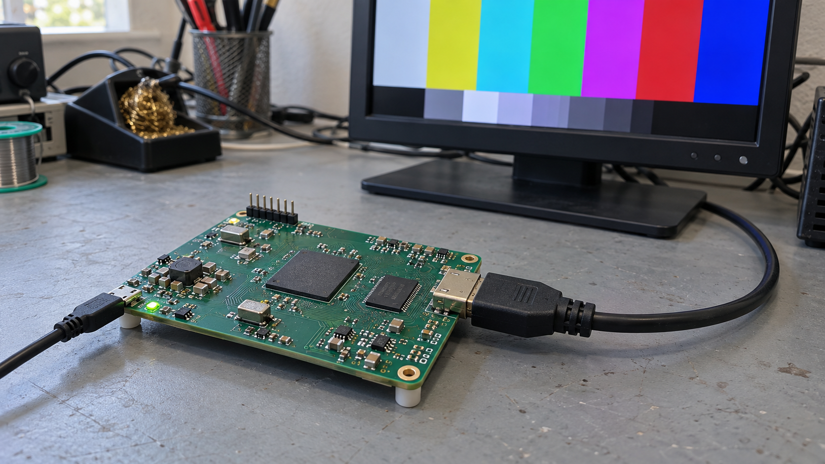
How a Verilog display controller turns pixel coordinates into a 720p video signal.
An FPGA display controller must do more than generate RGB values. It must deliver each pixel at the correct time, mark the active image area, and drive an output interface that the display can receive. Project F Display Controller provides a compact, open-source example of this process, with separate modules for clocks, video timing and DVI signal generation. [1, 2]
What the project demonstrates
Created by Will Green, the project includes Verilog examples for VGA and DVI output. Its DVI video can be used with compatible HDMI inputs, but the controller does not implement HDMI audio or advanced HDMI features. The repository includes test patterns and constraints for Arty and Nexys Video boards. These examples provide useful reference designs; a different board still needs its own clock, pin and electrical checks. [1]
Following one pixel through the design
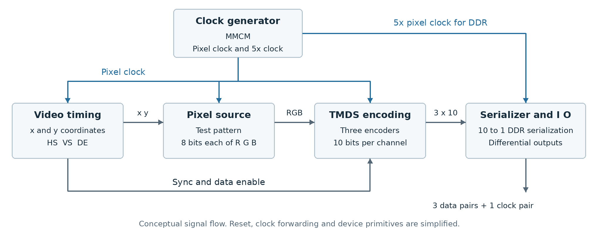
The timing module supplies pixel coordinates, horizontal and vertical synchronization, and data enable. The pixel source uses the coordinates to calculate a color. A procedural test pattern can therefore produce an image without storing a complete frame in memory. [2, 5]
For DVI output, three TMDS encoders convert the red, green and blue channel information into 10-bit symbols. The symbols are serialized and sent over three differential data pairs; a fourth pair carries the clock. The VGA path uses the timing and pixel information without this TMDS encoding stage. [2, 8, 9]
Calculating the 720p pixel clock
A 1280 × 720 picture contains 921,600 visible pixels, but the video timing also includes blanking intervals. The project’s 60 Hz 720p preset has 1,650 pixel periods per line and 750 lines per frame. The front porch, synchronization pulse and back porch make up the difference between the visible image and the complete raster. [3, 7]
| 720p timing | Active | Front porch | Sync | Back porch | Total |
|---|---|---|---|---|---|
| Horizontal periods | 1,280 | 110 | 40 | 220 | 1,650 |
| Vertical lines | 720 | 5 | 5 | 20 | 750 |
Pixel clock = 1,650 × 750 × 60 = 74,250,000 Hz = 74.25 MHz.
The serializer sends 10 bits for each pixel period on each data lane. It uses double data rate operation, so a clock running at five times the pixel rate produces a serial bit rate ten times the pixel rate. Keeping these quantities separate prevents a common mistake: treating the lane bit rate as the pixel clock. [3, 9]
| Project preset | Pixel clock | 5x DDR clock | Bit rate per data lane |
|---|---|---|---|
| 640 × 480 at 60 Hz | 25.2 MHz | 126 MHz | 252 Mbit/s |
| 800 × 600 at approximately 60 Hz | 40 MHz | 200 MHz | 400 Mbit/s |
| 1280 × 720 at 60 Hz | 74.25 MHz | 371.25 MHz | 742.5 Mbit/s |
These values describe the repository presets. They are not a substitute for checking the timing accepted by a particular display; alternative timing standards can use different pixel clocks. [3, 7]
What changes when you add a framebuffer
A generated color pattern is a useful first test because it separates basic video output from memory access. A framebuffer introduces another requirement: pixels must arrive continuously, even while other logic is using the memory.
For an uncompressed 1280 × 720 image with 24-bit RGB, one frame needs 1280 × 720 × 3 = 2,764,800 bytes, or about 2.64 MiB. Reading one complete frame 60 times per second requires about 165.9 MB/s of pixel payload. These are calculated values, not measured Project F performance. Memory overhead, arbitration and simultaneous writes require additional bandwidth; buffering must also handle the burstier consumption during active video.
Check the FPGA and board before adapting the design
This implementation uses Xilinx 7-series primitives. The clock generator relies on an MMCM, while native TMDS output uses OSERDESE2 serializers and OBUFDS differential buffers. Porting to a different FPGA family requires suitable replacements for those device-specific blocks, together with new timing and I/O constraints. [5, 6, 9, 10]
Nexys Video is one documented board target. Digilent lists its FPGA as XC7A200T-1SBG484C. That identifies a reference platform; it does not establish the minimum FPGA size for every video application. The resource and memory requirements depend on the logic added around the controller. [1, 11]
Before reusing the example, check the board oscillator, exact FPGA part and speed grade, available differential pins, I/O bank voltage and output circuit. Review the pin assignments and timing constraints, then check implementation reports against the required pixel and serializer clocks. A matching resolution alone does not demonstrate compatibility.
A practical first validation sequence
- Start with a repository preset and a simple test pattern. Match the clock configuration and pin constraints to the actual board.
- Verify reset and clock lock. The DVI demo holds downstream logic in reset until the clock generator reports lock. [5]
- In simulation, check the full line and frame counts and the active image area. Keep RGB data aligned with data enable and synchronization when adding pipeline stages.
- After checking implementation timing and electrical requirements, test the output on the intended display. Add framebuffers, camera input or image processing only after the basic path works.
Common questions
Does this provide a full HDMI transmitter?
No. It generates DVI-compatible video; the project does not provide HDMI audio or advanced HDMI features. [1]
Can I assume 1080p60 works on every 7-series board?
No. The README warns that direct TMDS serialization at 1080p60 is outside the stated 7-series specification. Evaluate the exact FPGA, speed grade and board implementation rather than treating the example as a universal operating guarantee. [1]
Can this code be used in another project?
The repository publishes its design and documentation under the MIT License. Preserve the required copyright and permission notice when distributing copies or substantial portions. Check any additional code or assets separately. [4]
Sources and scope
Project F Display Controller is by Will Green and Project F. This independent FPGAX article is based on a review of the public documentation and RTL listed in the source notes, accessed on 30 September 2026. FPGAX did not simulate or run this design on hardware for this article. The repository also points readers to a newer display controller in Isle. [1]
For Artix-7 sourcing inquiries, send the complete manufacturer part number, quantity and required delivery date to [email protected].