
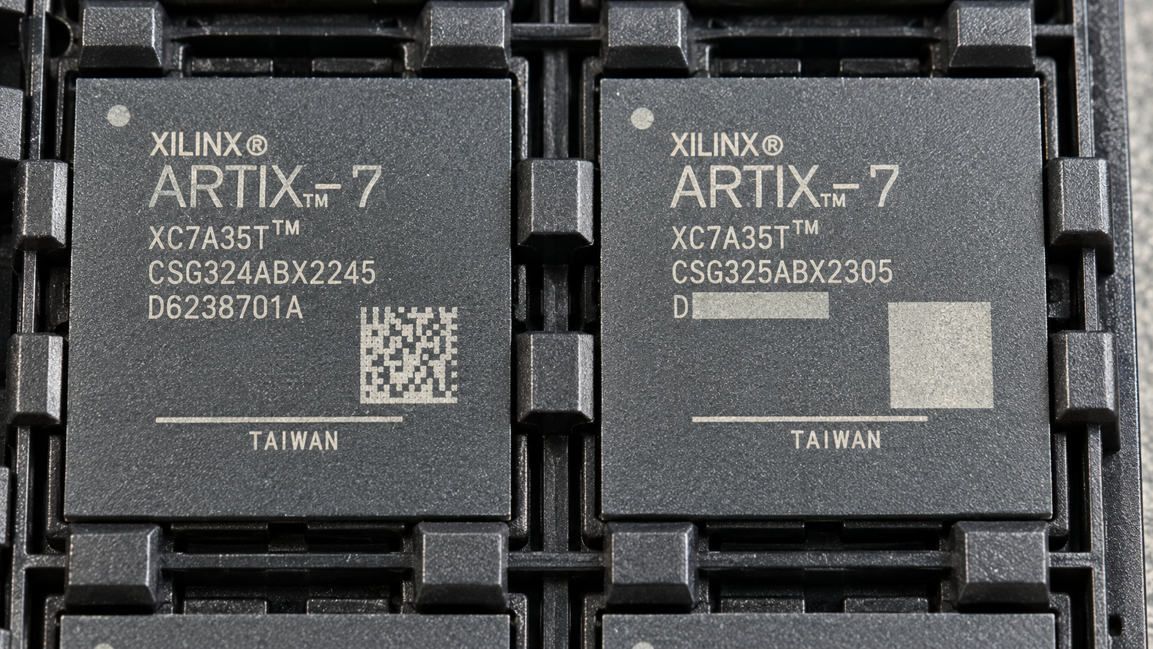
A package comparison with a reproducible check of all 324 ball positions
The XC7A35T in CSG324 cannot use its integrated PCIe block because the package does not bring out the GTP transceivers. CSG325 brings out four GTP channels, but it is not a drop-in replacement for CSG324. The two packages have different signal and power assignments. [1, 2, 4]
We compared AMD’s two XC7A35T pinout files by ball coordinate. Of the 324 positions in each file, 322 have different Pin Name entries. The differences include JTAG, configuration and supply pins. This article explains the selection consequences and identifies the official source files so you can check the result. [4]
The package changes the available interfaces
| XC7A35T package | CSG324 | CSG325 |
|---|---|---|
| Package body | 15 × 15 mm | 15 × 15 mm |
| Ball pitch | 0.8 mm | 0.8 mm |
| Positions listed in pinout | 324 | 324 |
| Maximum HR user I/O | 210 | 150 |
| Exposed GTP channels | 0 | 4 |
Table 1. XC7A35T package data from DS180 Table 5 and AMD’s package pinout files. HR means high-range I/O. GTP channels are counted separately from HR user I/O. [1, 4]
CSG325 exchanges some of the package’s user I/O availability for access to dedicated serial transceivers. It therefore does not improve every design. A design that needs many ordinary I/O signals and no GTP link may have different requirements from a PCIe endpoint.
Why the device overview is not enough
A device-level PCIe entry describes a block in the FPGA. Using that block also requires the appropriate transceivers to be connected through the selected package. PG054 explicitly uses XC7A35T in CSG324 as an example where this requirement is not met. [2]
This is a package limitation. Changing the HDL, buying a different IP license or moving the project to a newer Vivado release cannot add the missing package connections. The conclusion concerns the FPGA’s integrated PCIe path; it does not rule out a different system architecture with external bridge hardware.
Three ball positions explain the replacement risk
The practical question for an existing board is what each PCB pad will connect to after a substitution. The following examples use the exact names in AMD’s files. They show why a similar package outline is insufficient evidence of electrical compatibility. [4]
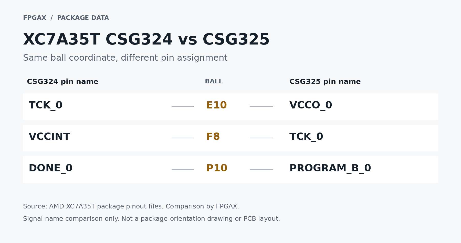
At E10, a PCB pad connected to the CSG324 JTAG clock would instead connect to VCCO_0 on CSG325. At F8, the CSG324 VCCINT location becomes the CSG325 JTAG clock. At P10, DONE_0 becomes PROGRAM_B_0. These changes cannot be corrected by merely editing the FPGA pin constraints; the board connections also have to match the selected device.
Power differences extend beyond those examples. A2 is GND in CSG324 and MGTAVTT in CSG325. A replacement review must include supply and ground connections, even for signals the application does not use. [4]
What the 322 count means
The count is an exact comparison of the Pin Name strings at the same ball coordinates after trimming surrounding whitespace. It is not a count of 322 independent electrical hazards. Two different user-I/O names and a signal-to-supply change both count as different, although their implications are very different.
Only H3 and V17 retain identical Pin Name entries in the two files. That does not establish a safe partial replacement. Use the complete comparison and the actual board netlist when assessing a proposed change. [4]
CSG325 still requires the right speed grade
Four exposed GTP channels do not make every XC7A35T-CSG325 ordering option suitable for every PCIe configuration. PG054 lists Artix-7 support for x1, x2 and x4 links, and its Core Configurations table specifies the supported speed grades. [3, 5]
| PCIe configuration | Artix-7 speed grades listed in PG054 |
|---|---|
| Gen1 x1, x2 or x4 | -1, -2, -3, -2L |
| Gen2 x1, x2 or x4 | -2, -3 at 1.0 V VCCINT |
Table 2. Artix-7 entries in PG054 v3.3, Minimum Device Requirements, Table 1. Package availability and the exact ordering option must also be checked. [3]
For a Gen2 design, do not approve a -1 part merely because its package is CSG325. Confirm the complete part number and the IP configuration against the documentation for the tool version being used. The board also needs the required transceiver supplies, reference clock and serial routing.
A selection check before buying or changing the BOM
- Record the complete ordering code. Keep the device, speed grade, package and temperature suffix in the quotation, purchase order and BOM. “XC7A35T” alone is not enough to identify the required part.
- State the interface requirement. For an integrated PCIe design, record the generation and lane width. For other designs, record the required user I/O, bank voltages, clocks and any GTP links.
- Compare the proposed package with the schematic and PCB. Review power and ground first, then configuration and JTAG, clocks, transceivers and user I/O. Check the full pin names and bank assignments, not only the total I/O count.
- Retarget and implement the design. Select the exact part in Vivado, regenerate the relevant IP and constraints, and examine the design-rule and timing reports. A successful synthesis alone does not demonstrate that a board is correctly wired.
- Record who approved the change and what was checked. Keep document versions, the pin comparison and implementation results with the change record. For an existing CSG324 board, treat a move to CSG325 as an engineering change requiring board review.
A useful instruction for a supplier
Quote the exact manufacturer part number shown in the BOM. Identify any proposed alternative separately, including its package and speed grade. Do not ship an alternative until the customer has approved the engineering change.
How to reproduce the pinout comparison
We downloaded the Artix-7 package archive from AMD on 2 October 2026 and selected xc7a35tcsg324pkg and xc7a35tcsg325pkg. Each package has a CSV and a TXT representation. The script checks for duplicate or missing ball coordinates and compares all eight fields between the CSV and TXT versions before producing the cross-package comparison.
Both files contain the same set of 324 coordinates. The CSV and TXT records agree within each package. The source records include pin names, banks, I/O types and memory byte groups. Use the original AMD files linked below when repeating the comparison. [4]
Download the original pinout files from AMD’s Artix-7 package pinout page. Select xc7a35tcsg324pkg.csv, xc7a35tcsg324pkg.txt, xc7a35tcsg325pkg.csv and xc7a35tcsg325pkg.txt. Match rows by ball coordinate and compare the Pin Name fields after trimming surrounding whitespace. Check for duplicate or missing coordinates before interpreting the result. [4]
Questions that affect the decision
Does CSG325 mean 325 balls?
Not for these XC7A35T files. AMD’s CSG324 and CSG325 files each declare and list 324 positions. Treat the suffix as a package identifier, rather than inferring a one-ball difference. [4]
Should every new XC7A35T design use CSG325?
No. Select it when its exposed interfaces and I/O allocation fit the design. CSG324 provides more HR user I/O in this comparison; CSG325 provides GTP access. [1]
Can this comparison approve a substitute for my board?
No. It identifies documented differences. Approval needs the actual schematic, PCB, power design and FPGA implementation, followed by appropriate hardware validation.
Sources and scope
This FPGAX article reports a document review and an executed comparison of AMD pinout data. AI tools assisted the research and drafting. No Vivado implementation, signal-integrity measurement or hardware PCIe test was performed for this article. The results apply to the named XC7A35T files and should not be extrapolated to every Artix-7 device.
References
- AMD DS180 v2.6.1, 8 September 2020, page 3, Tables 4 and 5
- AMD PG054 v3.3, 6 December 2024, Available Integrated Blocks for PCIe
- AMD PG054 v3.3, Minimum Device Requirements, Table 1
- AMD Artix-7 package pinout files, downloaded 2 October 2026
- AMD PG054 v3.3, Artix-7 Devices, recommended GT locations
For an Artix-7 sourcing inquiry, send the complete manufacturer part number, quantity and required delivery date to [email protected]. Please identify proposed alternatives separately from the approved BOM part.