
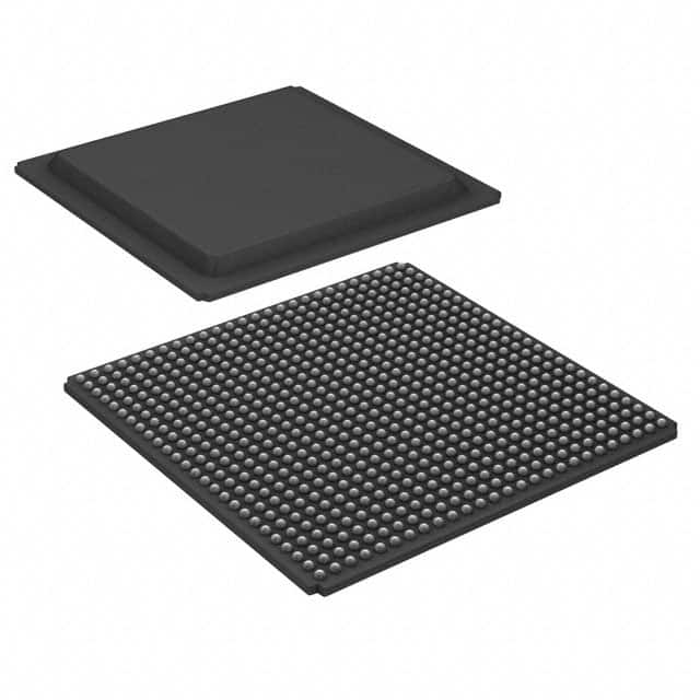
XCKU5P-L1FFVB676I
AMDKintex UltraScale+ FPGA with 474,600 logic cells and 280 user I/O in a 676-ball flip-chip BGA, industrial temperature range.
- Part Number
- XCKU5P-L1FFVB676I
- Manufacturer
- AMD
- Series
- Kintex® UltraScale+™
- Logic cells
- 474,600
- User I/O
- 280
- Package
- 676-FCBGA (27x27)
- Temperature
- Industrial, -40°C to 100°C (TJ)
- Datasheet
- XCKU5P-L1FFVB676I.pdf


Request a Quote
Get confirmed pricing, availability and lead time.
How to read XCKU5P-L1FFVB676I
Each part of the number carries one specification. Read from left to right: device, speed grade, package and temperature grade.
Specifications
| Series | Kintex® UltraScale+™ |
|---|---|
| Logic cells | 474,600 |
| CLBs | 27,120 |
| Total RAM bits | 41,984,000 |
| User I/O | 280 |
| Supply voltage | 0.698V to 0.876V |
| Speed grade | -L1 |
| Operating temperature | Industrial, -40°C to 100°C (TJ) |
| Package | 676-FCBGA (27x27) |
| Package / case | 676-BBGA, FCBGA |
| Mounting | Surface Mount |
| Lifecycle | Active |
Values follow the manufacturer's published data. Confirm against the data sheet before design-in.
Documents
- Manufacturer data sheet for XCKU5POpens on docs.amd.com
About the Kintex UltraScale+ family
Kintex UltraScale+ is a Xilinx (now AMD) FPGA family. The 7 devices listed on this site range from 355,950 to 1,842,750 logic cells.
Questions buyers ask about XCKU5P-L1FFVB676I
Is XCKU5P-L1FFVB676I still in production?
Yes. The manufacturer lists it as an active part.
How many user I/O pins does XCKU5P-L1FFVB676I have?
280, in the 676-ball flip-chip BGA package. The same device in another package has a different I/O count.
How is the price for XCKU5P-L1FFVB676I set?
By quote. Prices for programmable logic move with supply, so we confirm price and lead time for your quantity when you send a request.
Other versions of XCKU5P
The same device is listed in other packages, speed grades and temperature grades. Each is a different part number, so match the full number on your bill of materials.
| Part number | Speed grade | Package | User I/O | Temperature |
|---|---|---|---|---|
| XCKU5P-1FFVB676E | -1 | 676-FCBGA (27x27) | 280 | 0°C to 100°C (TJ) |
| XCKU5P-1FFVB676I | -1 | 676-FCBGA (27x27) | 280 | -40°C to 100°C (TJ) |
| XCKU5P-2FFVB676E | -2 | 676-FCBGA (27x27) | 280 | 0°C to 100°C (TJ) |
| XCKU5P-2FFVB676I | -2 | 676-FCBGA (27x27) | 280 | -40°C to 100°C (TJ) |
| XCKU5P-3FFVB676E | -3 | 676-FCBGA (27x27) | 280 | 0°C to 100°C (TJ) |
| XCKU5P-L2FFVB676E | -L2 | 676-FCBGA (27x27) | 280 | 0°C to 100°C (TJ) |
| XCKU5P-1FFVA676E | -1 | 676-FCBGA (27x27) | 256 | 0°C to 100°C (TJ) |
| XCKU5P-1FFVA676I | -1 | 676-FCBGA (27x27) | 256 | -40°C to 100°C (TJ) |
| XCKU5P-2FFVA676E | -2 | 676-FCBGA (27x27) | 256 | 0°C to 100°C (TJ) |
| XCKU5P-2FFVA676I | -2 | 676-FCBGA (27x27) | 256 | -40°C to 100°C (TJ) |
| XCKU5P-3FFVA676E | -3 | 676-FCBGA (27x27) | 256 | 0°C to 100°C (TJ) |
| XCKU5P-L1FFVA676I | -L1 | 676-FCBGA (27x27) | 256 | -40°C to 100°C (TJ) |
| XCKU5P-L2FFVA676E | -L2 | 676-FCBGA (27x27) | 256 | 0°C to 100°C (TJ) |
| XCKU5P-1FFVD900E | -1 | 900-FCBGA (31x31) | 304 | 0°C to 100°C (TJ) |