FPGA Replacement Checklist: What to Verify Before Changing a Part
An FPGA replacement needs approval for a specific board and design. A matching package code or a larger logic count is only a starting point. The useful question is whether the proposed device can meet your electrical, implementation and system requirements.
Keep two statuses in your sourcing records: procurement candidate and engineering-approved replacement. A quotation can identify a candidate. Release it for substitution only after your engineering team has accepted the evidence below.
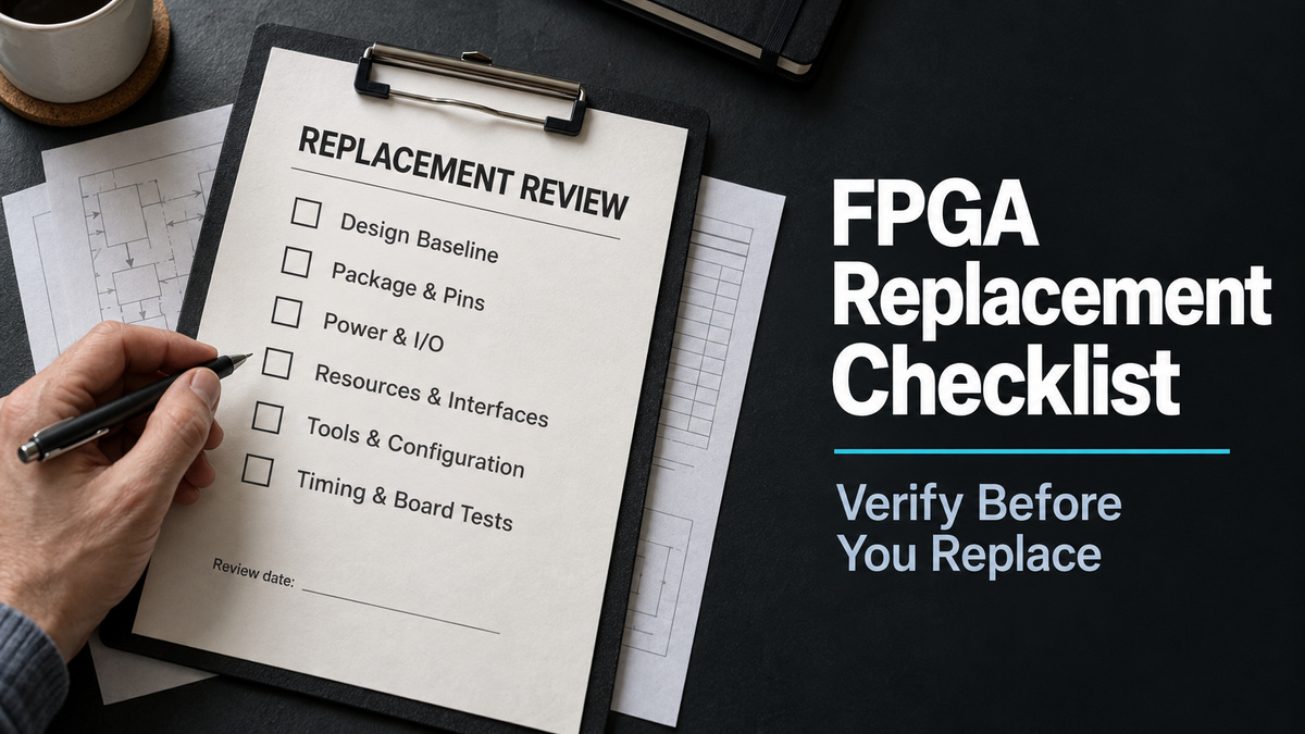
1. Freeze the original design baseline
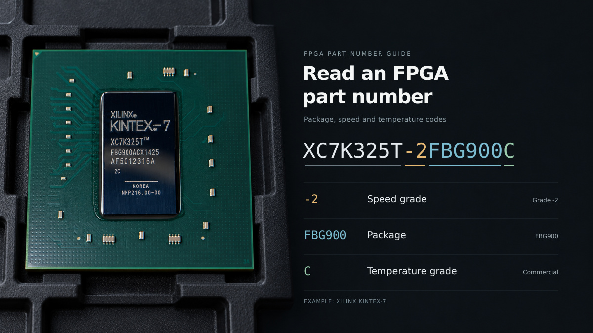
Record the complete original and proposed ordering codes, including package, speed grade and temperature grade. Attach the board revision, schematic revision, FPGA project revision and production programming-file identifier.
Have the engineer list what the design actually uses: logic, memory and DSP resources; I/O assignments; clocks; serial links; and required hard blocks or licensed IP. Compare requirements against the exact target device and package. A family-level feature list is not enough to approve a particular ordering code.
Preserve the working project before changing the target. This gives the team a reproducible baseline and a way to distinguish migration changes from unrelated fixes.
2. Prove the pin migration path
Compare the official pinout files and package drawings against the board netlist. Review every package pin or ball, including power, ground, reserved and no-connect positions. Save a differences table showing the board connection, original function, proposed function and resolution.
AMD's 7 series packaging guide warns that same-package migration can change bank assignments and clock-capable or differential pin functions. It also notes that pin-compatible packages can require substantially different decoupling. Those statements apply to the documented 7 series combinations; they do not establish compatibility across unrelated families. AMD UG475, v1.20, “Migrating between Devices”
For supported Altera targets, use the migration checks in the applicable Quartus edition and family documentation. The Quartus Prime Pro guide describes the Pin Migration Window and warns that PCB power or ground connections still need review. Archive the report with the schematic comparison. Altera, Design Constraints, v25.1.1
For the specific Artix-7 package question, see our XC7A35T CSG324 versus CSG325 discussion.
3. Recheck power and every used I/O bank
Make a rail-by-rail comparison of operating voltage, regulator capacity, startup requirements and decoupling. Use the proposed device's data sheet for sequencing. AMD's design methodology directs designers to that device-specific source. AMD UG949, “Power Supply Paths on Devices”
For each connected interface, record the I/O standard, bank supply, reference voltage and termination. Check the receiving device's requirements too. AMD's 7 series SelectIO guide distinguishes bank support and VCCO/VREF requirements by I/O standard; its tables must not be applied to other architectures. AMD UG471, v1.10, Table 1-55
Include power and thermal estimates for the actual workload. Flag any regulator, cooling or PCB change before procurement treats the candidate as usable.
4. Check clocks, transceivers and hard blocks
Trace each board clock to its proposed input pin and internal clock resources. Record required frequencies, clock relationships and reset behavior.
For serial links, compare the transceiver type, usable channel locations, line rate, reference-clock access and relevant protocol IP. AMD's 7 series Transceivers Wizard exposes available channels according to the selected device and package, alongside line-rate and clock settings. A headline transceiver count therefore needs a package-specific check. AMD PG168, v3.6, “Line Rate, Transceiver Selection, and Clocking”
Have engineering document how every required hard block and interface maps to the target. Treat unresolved mappings as open issues.
5. Establish the build and configuration path
Confirm that the chosen tool release supports the exact target and that the project has the required source files, IP versions and licenses. In Vivado, review Report IP Status after a part change. AMD documents part-change status and recommends archiving the project before IP upgrades, which remove previously generated output products. AMD UG896, 2026.1, “Upgrading IP”
Require a reproducible build for the proposed target, with reviewed pin and timing constraints. Preserve the tool version, build logs and programming-file identifier.
Do not assume the production bitstream transfers unchanged. For 7 series devices, configuration includes a device-ID check to prevent loading a bitstream formatted for a different device. Also review boot mode, configuration-pin voltages, flash capacity and startup behavior against the target's configuration guide. AMD UG470, v1.17, Chapters 1 and 5
6. Close timing and validate the board
Review synthesis and implementation results, resource use, design-rule checks and setup/hold timing. Inspect unconstrained paths and timing exceptions before accepting a passing summary. AMD's methodology calls for checking synchronous endpoints and reviewing timing constraints with check_timing and report_methodology. AMD UG949, 2026.1, “Checking That Your Design is Properly Constrained”
Then execute an engineering-approved hardware test plan on the intended board revision. A useful proposed scope includes repeated boot and reset, memory and interface traffic, application workloads, and relevant voltage and temperature conditions. Record acceptance limits before testing. A successful configuration or brief bench demonstration should not be the entire acceptance record.
A worksheet to attach to the change request
Use one record per original/proposed part pair. Add an evidence link, reviewer and status to each row.
| Review area | Evidence to attach |
|---|---|
| Identity and design baseline | Full ordering codes; board and project revisions |
| Package and pins | Official pinouts; net-by-net differences; migration report |
| Electrical and thermal | Rail/I/O comparison; power and cooling review |
| Resources and interfaces | Utilization; clock, transceiver and hard-block mapping |
| Tools and configuration | Tool/IP/license record; build log; boot-file details |
| Acceptance and release | Timing review; hardware test results; signed change record |
Use open, passed, failed or not applicable with reason. Keep unresolved candidates out of the approved substitution list. Tie approval to the tested board, project and programming-file revisions.
When you request a sourcing quote from FPGAX, include the original part, quantity, required date and any proposed alternative. State whether engineering has approved that alternative or is still evaluating it. Complete engineering approval before authorizing substitution.