FPGA Configuration Memory: Questions to Resolve Before Ordering
Choose FPGA configuration memory from a documented boot design. The FPGA ordering code, boot mode and approved programming image should lead the decision. A configuration-bit count alone cannot identify a suitable flash part.
Before requesting a quotation, ask engineering for a memory approval record. It should identify what the memory does, how much address space the released images occupy and which exact parts the board and programming process support.
Establish the configuration architecture
First determine where the device retains its configuration and how the intended board starts. For the FPGA architectures covered by AMD UG570, configuration must be reloaded after a power cycle. The guide describes loading from external memory or another system device. Its scope does not cover every FPGA architecture. AMD UG570, v1.20.1, Overview
Microchip's PolarFire family uses nonvolatile FPGA technology. Its programming guide nevertheless requires external SPI flash for the documented in-application programming and auto-update flows. Retaining the FPGA configuration and storing an update image are separate functions. Microchip DS50003191L, Introduction and Chapter 11
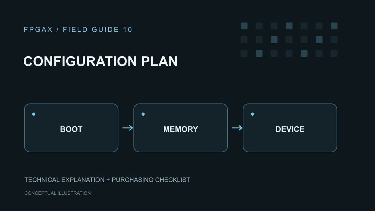
Create a simple boot diagram showing the FPGA, any controller and each memory device. Label the role of each stored image. Include processor software where the system has a processor boot flow, and identify the guide governing that flow.
This diagram should answer a practical purchasing question: is the requested memory needed for ordinary startup, field updates, application storage or several of those tasks? Record the answer before comparing memory densities.
Build an address map from the released files
Ask for the actual generated programming files and their layout. Record each image's name, version, start address and reserved region. Identify any recovery image and decide where future updates may be stored.
Keep image size and allocated space as separate fields. A layout may reserve a region larger than the present file. Have engineering account for alignment, erase boundaries and any metadata required by the chosen implementation. Use the relevant memory and configuration documents to resolve these details.
Check units throughout the record. Keep bit counts, byte counts and the memory supplier's stated density visibly labelled. If a sizing calculation uses a conversion or rounding step, show it so another engineer can reproduce the result.
Avoid approving a flash from a compressed build that happens to fit today. Ask what image options, recovery provisions and approved growth allowance define the capacity requirement. The resulting allocation should become part of the design release, with changes reviewed alongside the programming files.
Review the exact memory interface
Record the full memory ordering code, package and voltage variant. Compare its pinout and supply requirements with the schematic. Include the FPGA configuration-bank supply and any shared devices on the bus.
Ask engineering to confirm the selected boot controller's command and addressing compatibility with the memory. Record the applicable clock limit and the source establishing it. If the same memory is accessed after configuration, document how ownership of the interface changes.
Check startup assumptions explicitly. Which component becomes ready first? What state must the mode pins and chip-select signals have? Does the design require a particular power-up command sequence? Attach the reviewed timing or sequence diagram instead of relying on a generic “SPI compatible” description.
A proposed memory substitution should reopen this record. Matching package size and density are useful search filters, but the electrical and command details still need an engineering decision.
Check programming support separately from boot support
Find the memory in the appropriate programming-tool documentation for the FPGA family and tool release. AMD's UG908 memory tables describe devices the software can erase, program and verify; listing does not assure present or future supply. AMD UG908, 2026.1, Kintex 7 Configuration Memory Devices
Keep this tool check separate from the board's boot review. Record how blank memories will be programmed, which equipment will be used and whether the procedure also covers recovery or service work.
For an external programming service, define the delivered file, address offsets and required operations. Confirm that the receiving party can interpret the release package before authorizing a production quantity. Do not assume that a design file and a manufacturing programming file serve the same purpose.
Define programming and startup acceptance
Write down what a successful programming operation proves and what the board test must establish. UG908 distinguishes programming from verification against the configuration file. Its described workflow also lets the user select the address range affected. AMD UG908, 2026.1, Programming a Configuration Memory Device
Specify the required operations in the work instruction. Preserve the result, file identifier and target-memory identity. Then test normal startup using the released boot path, rather than relying solely on a development cable.
Have engineering set acceptance conditions for repeated startup, interrupted updates and recovery where those behaviors are part of the product requirements. Record expected outcomes before testing. This article does not prescribe universal test limits or imply that one successful boot establishes production readiness.
A configuration-memory approval record
Use the following proposed checklist for the FPGA and memory pair. Add the evidence location, reviewer and approval date.
| Field | Information to retain |
|---|---|
| Target design | FPGA ordering code, board revision and project revision |
| Memory role | Startup, update, recovery or application-storage purpose |
| Boot path | Mode selection, controlling device and applicable guide |
| Image layout | Released files, offsets, allocated regions and capacity calculation |
| Electrical review | Memory variant, pinout, supply and startup requirements |
| Interface review | Commands, addressing, clock settings and bus ownership |
| Programming process | Tool release, programmer, supported target and work instruction |
| Acceptance record | Programming verification, board boot results and unresolved items |
Mark unknowns as open. If the recovery method is undecided or the tool cannot identify the proposed memory, return the item to engineering before purchase approval.
For an FPGA sourcing request to FPGAX, include the complete approved FPGA code and explain whether configuration-memory choices are fixed. Keep any proposed component alternative subject to the same documented review.