FPGA Transceivers and GPIO: Check the Interface Your Design Needs
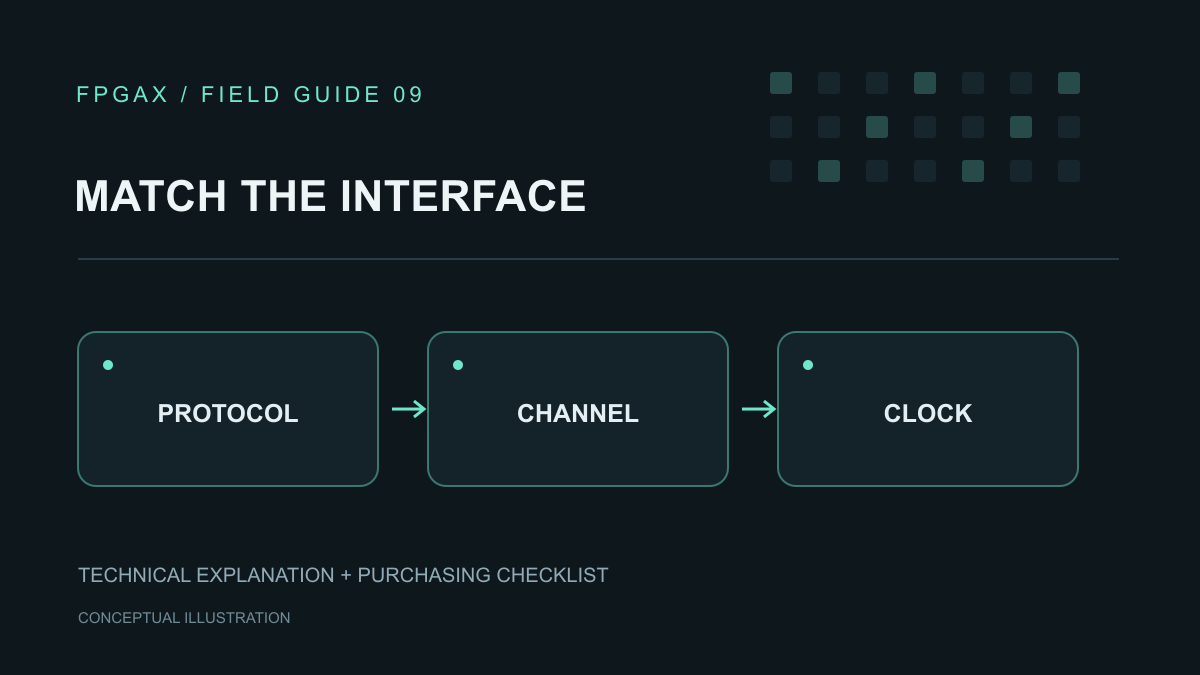
An FPGA interface requirement should identify the connection the board must make, the resources it needs and the evidence supporting the selected part. A headline GPIO count or transceiver count leaves too many questions open for purchasing.
Start with one record per external interface. Have engineering complete it before the part becomes an approved BOM item. This makes it easier to explain why a package, speed grade or apparently similar device cannot be substituted without review.
Separate GPIO, transceivers and protocol logic
Keep general-purpose I/O and dedicated serial transceivers in separate resource columns. AMD's 7 series Transceivers Wizard configures on-chip transceivers; its available channels depend on the selected device and package. A user-I/O total therefore cannot stand in for a usable transceiver allocation. AMD PG168, v3.6
For a parallel interface, record the signals, electrical standard, bank allocation and timing requirements. For a serial link using dedicated transceivers, record the transmit and receive channels, reference clock and required physical-layer settings. Keep sideband control signals in the GPIO budget even when the main data path uses transceivers.
Then identify the protocol implementation. AMD's 7 series PCIe guide has separate requirements for device resources, clocking and the integrated protocol block. Having a serial channel does not establish a complete PCIe implementation. AMD PG054, v3.3, Minimum Device Requirements
This distinction matters when a quotation says “PCIe capable.” Ask engineering to turn that description into a specific, documented configuration before accepting the part.
Describe the link before choosing the chip
Write down the protocol and revision, endpoint role, lane count, required line rate and intended connection partner. Separate application payload demand from the electrical link settings. Ask engineering to show how the selected protocol mode meets the workload, including its traffic pattern.
Record which requirements are fixed by the existing board and which can change. An established connector pinout may be fixed; the internal data-path width might still be a design choice. Keeping these categories separate prevents a purchasing discussion from silently becoming a board redesign.
For custom links, attach the interface specification. “High-speed serial” is not a sufficient requirement. State the expected encoding, framing, error handling and startup behavior, with an owner responsible for each open decision.
Prove that the selected package exposes the resources
Create a channel map for the exact ordering code. Connect each required lane to an internal channel location and then to the package balls and board nets. Review both transmit and receive directions, including any unused direction.
Keep the package pinout and the tool's selected target with this map. Treat a family overview as an initial filter. Before approval, require evidence that the actual device/package combination exposes the channels the layout uses.
Include the relevant hard-block location and routing restrictions in engineering's review. Ask whether the selected protocol implementation can reach the planned channels. A drawing with enough differential pairs is incomplete until those connections are checked against the target architecture.
For a concrete package discussion, see the existing XC7A35T CSG324 versus CSG325 article. Its conclusions should stay within the specific devices and packages discussed.
Trace the reference clock and reset path
Draw the clock path from its source through any buffer to the FPGA pins. Record frequency, electrical format and the applicable jitter requirements. Reference-clock choices are explicit settings in the 7 series Transceivers Wizard. Check them against the chosen channel allocation. AMD PG168, v3.6
Ask the designer to resolve shared-clock dependencies before the schematic is frozen. List any other links using the same clock source or shared resources. Document what happens when one link resets, loses its reference or changes operating mode.
Keep boot and reset assumptions in the interface record. Identify who releases reset, what must already be stable and what evidence confirms that sequence. A passing data-sheet comparison cannot establish the behavior of the assembled board.
Check IP, tools and the actual board path
Record the protocol core name, version, selected features and licensing basis. For example, PG054 v3.3 states that its documented 7 series PCIe core is provided with Vivado at no additional cost under the applicable license. That statement does not establish the terms of other cores. AMD PG054, Licensing and Ordering
Preserve the generated IP configuration and the supported tool release. Have engineering build the proposed target with the intended constraints and retain the relevant implementation reports.
The board review should also cover the connector, routing, coupling components and link partner. Assign responsibility for checking each against the interface's electrical requirements. Record the planned hardware acceptance method and limits before testing. A linked example design is useful evidence of a starting point; your board still needs its own acceptance record.
Use an interface approval worksheet
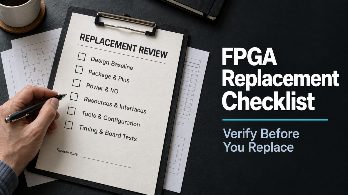
The following is a proposed internal worksheet, rather than a manufacturer-mandated form. Add an evidence location, reviewer and status to each row.
| Record | Question the evidence must answer |
|---|---|
| Interface requirement | What protocol, role, lanes and operating modes are required? |
| Resource allocation | Which signals use GPIO, dedicated channels or protocol blocks? |
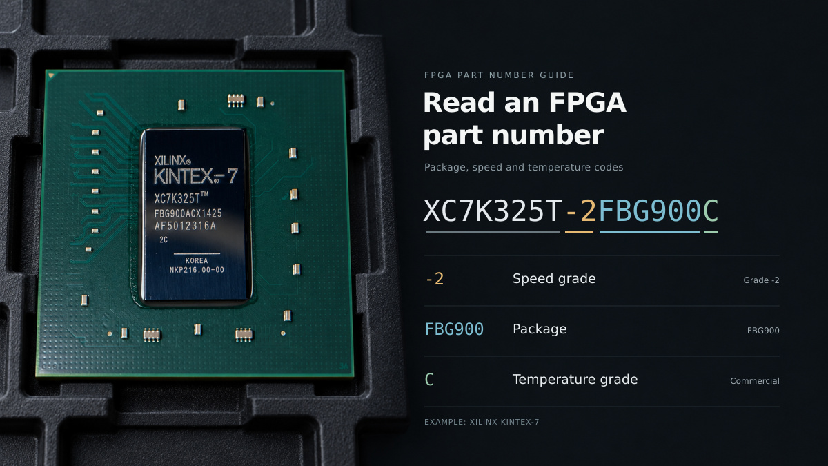
| Exact target | Which ordering code, package and speed grade were reviewed? |
| Channel and pin map | Where does each lane connect internally and on the board? |
| Clock and reset | Which sources and sequences support the intended operation? |
| IP and build | Which core configuration, tool release and license basis apply? |
| Board acceptance | What test conditions, limits and results support release? |
Use “open,” “accepted,” “rejected” or “not applicable with reason.” An unchecked family feature should remain open. Keep the record tied to the board revision and project revision so later changes are visible.
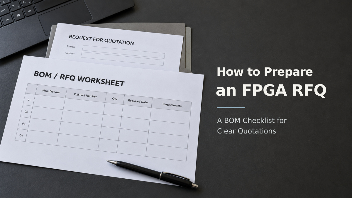
When you send an FPGA RFQ to FPGAX, provide the complete approved ordering code, quantity and required date. If alternatives may be considered, identify the interface constraints and state that engineering review is still required before substitution.