FPGA I/O Banks and Voltage: What to Check Before Choosing a Package
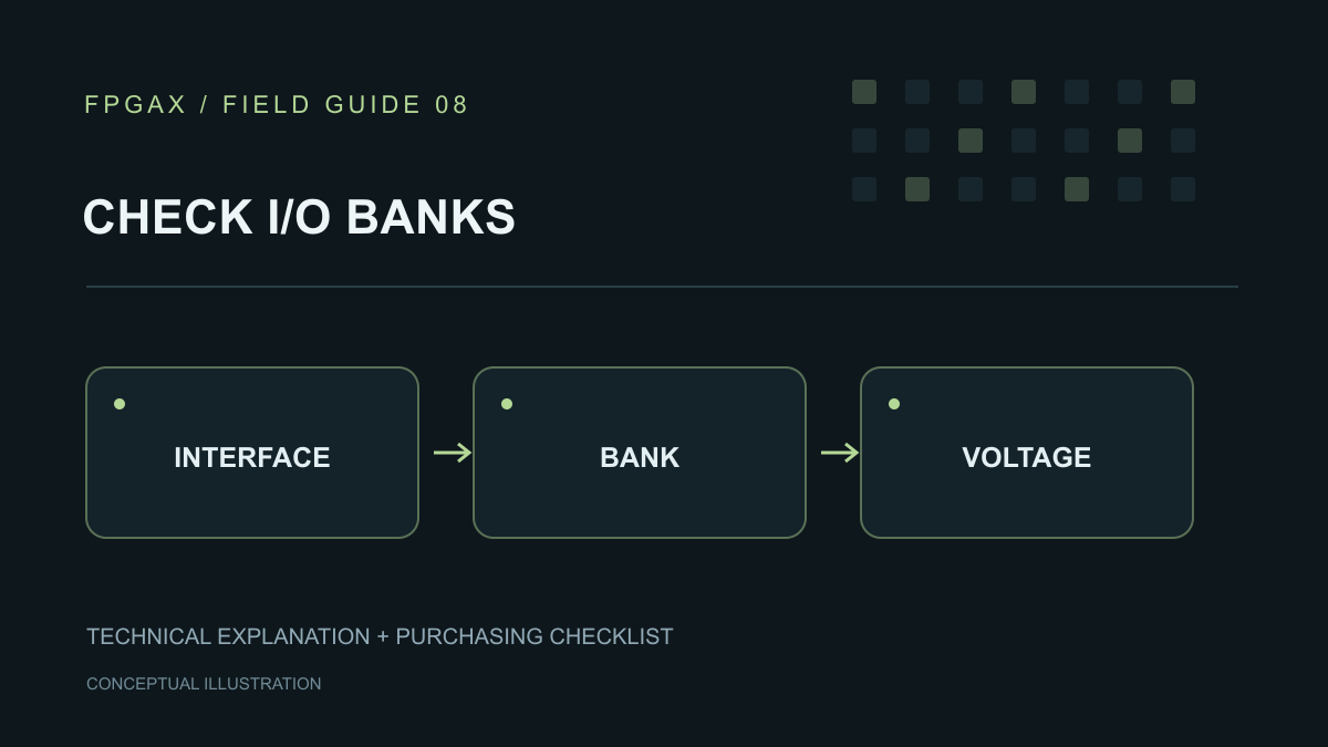
Choose an FPGA package after checking how the board's interfaces can be assigned to its I/O banks. Total user-I/O count is a useful screening field, but the review also needs signal direction, electrical standard, bank supplies and special pin functions.
Build an interface-to-bank matrix before approving a package. The proposed workflow below makes those requirements visible to both purchasing and engineering. The numerical examples from AMD 7 series and Altera Cyclone V apply only to their stated families.
Start from the devices connected to the FPGA
List every external interface, including control signals and programming connections. For each group, record the other device's exact identity and the relevant electrical specification.
Define direction from the FPGA's perspective. Keep inputs, outputs and bidirectional signals distinguishable. Add the number of signals or differential pairs, required data rate and any associated clock.
Record behavior outside normal operation too. Ask what happens while either component is unpowered, held in reset or being programmed. Give unresolved electrical questions an owner before committing signals to pins.
This step prevents a shorthand label such as “3.3 V interface” from becoming the entire requirement. The engineer needs to know which device drives, which receives and which conditions must be checked.
Identify the bank type and supply
For AMD 7 series, HP banks support I/O standards up to 1.8 V, while HR banks extend to 3.3 V. Check the bank types available in the selected device and package. AMD UG471, v1.10, I/O Tile Overview
Keep that family example separate from the review template. Another architecture can use different bank names, electrical capabilities and placement rules. Return to its own I/O guide when changing families.
For each proposed bank, record the board net supplying it and the intended voltage. Place the required I/O-standard name beside each signal group. Ask engineering to confirm the assignment against the data sheet and tool settings.
Review groups together. When one interface changes, reopen the assignments that share its bank instead of checking only the changed pin. Preserve the previous bank plan so the reason for a reassignment remains clear.
Treat reference voltage and termination as design choices
Give the bank supply, receiver reference and termination settings separate fields. Do not combine them into one “I/O voltage” column.
For Cyclone V, the handbook states that each bank has one VCCIO level and one VREF level. It also describes conditions for mixing voltage-referenced inputs, including different restrictions when on-chip termination is enabled. Altera Cyclone V handbook, Voltage-Referenced I/O Standards
For LVDS inputs, UG471 Table 1-55 makes differing-VCCO operation conditional on DIFF_TERM and device-specific VIN, VIDIFF and VICM limits. Internal differential termination requires the relevant output-standard VCCO level. AMD UG471, Table 1-55 and notes
The practical review action is to record the selected condition explicitly. For a differential input, ask engineering to document common-mode voltage, differential swing and termination location. Check both ends of the connection against their respective specifications.
If a note permits a special case, retain the note's conditions with the approval. A reference to the table without its exception criteria is incomplete evidence.
Use a matrix before assigning ball numbers
The rows below are a hypothetical planning example. They describe information to collect and do not prescribe a valid bank or package.
| Interface group | Known requirement | Information still needed before assignment |
|---|---|---|
| Control outputs | 12 signals, nominal 3.3 V signaling | Receiver limits, chosen I/O standard, bank supply and startup state |
| Parallel data bus | 16 bidirectional signals, nominal 1.8 V | Direction control, timing, drive settings and compatible bank |
| Differential receiver | Four input pairs | Exact standard, common-mode/swing limits, termination and clocking |
| Programming connection | Board access required after assembly | Selected mode, reserved pins and applicable electrical conditions |
Expand each row into individual signals when preparing the pin plan. Add proposed bank, package ball, reference-voltage source and review status. Keep the other device's limits visible rather than copying only an interface name.
Use “pending” for information that has not been established. A blank termination field should trigger a question, not an assumption that termination is unnecessary.
Confirm package access and special functions
Retrieve the pinout for the exact device/package combination. Altera's manufacturer directory organizes pinout files by device family and device, providing a starting point for that selection. Altera pinout directory
Ask engineering to check the functions required by each proposed assignment. Include differential pairing, clock access and interface-specific placement rules. Reserve configuration and other dedicated functions before calling the remaining pins available.
Check the schematic and footprint against the same revision of the pin plan. When a package changes, repeat this review even if its outline looks familiar. For an existing package-specific discussion, see XC7A35T CSG324 versus CSG325.
Reconcile the tool project with the board
Enter the intended part, pin assignments and electrical settings into the design project. In Vivado, the I/O planning environment includes I/O design-rule checks and simultaneous-switching-noise analysis. AMD UG892, 2026.1, I/O and Clock Planning
Save the reports with the matrix. Investigate warnings and errors, and record the disposition of each relevant issue. Then compare the project's settings with the actual rail connections and termination components in the schematic.
Treat tool results as one evidence item. Engineering should also define the board-level measurements needed for the implemented interface. Record the accepted operating conditions and the board revision to which approval applies.
Give purchasing an exact package decision
The handoff should name the complete ordering code, approved package and board revision. Attach the reviewed matrix and identify any remaining engineering conditions.
For a quotation request to FPGAX, include quantity, required date and the exact approved code. If a package alternative is still being evaluated, label it separately. Obtain engineering approval of its bank and pin assignments before allowing substitution.